
A research team led by Prof Goki EDA from the Departments of Physics and Chemistry, NUS has succeeded in developing highly energy efficient ultra-thin LEDs that comprise only a few layers of atoms. An efficient LED device converts most of its electrical power input into light emission (i.e. with minimal losses due to conversion into other forms of energy such as heat). Previous studies on LEDs based on 2D semiconductors reported that a large amount of electrical current is needed to trigger light emission. This means that a substantial fraction of the input electrical power is dissipated as heat instead of generating light. The team discovered that this energy loss can be significantly reduced by preventing the leakage of electrical current from the emissive layer to the metal electrodes. The researchers demonstrated that an insulating layer of a few nanometers can significantly suppress the loss of input electrical energy without introducing excessive electrical resistance. Quite the contrary, by optimising the thickness of the insulating layers, the team reduced the electrical current needed for triggering light emission by more than 10,000 times as compared to the state-of-the-art LEDs based on 2D semiconductors.
Prof Eda said, “Our devices can operate at extremely low electrical current because the device design ensures that there is minimal wastage of electrical power.”
“By optimising the material quality together with device design and fabrication methods, it becomes possible to have efficient light emission with precise control at the nanoscale level. This will potentially have significant impact on the development of future information technologies,” added Prof Eda.
The team is currently investigating the origin of energy loss processes in detail to further improve the efficiency of their devices.
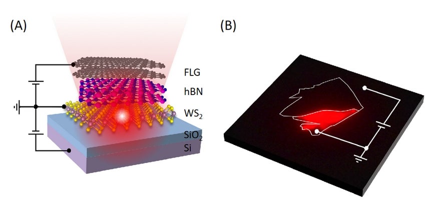
Figure shows the emission of red light from an electrically excited LED fabricated with 2D semiconductor materials. (A) The left image illustrates the device structure consisting of various layered materials. The stack of layers consist of few-layer graphene (FLG), hexagonal boron nitride (hBN) and tungsten disulfide (WS2). (B) The right image shows a microscope image taken in the dark while a voltage is applied to the device.
Reference
Wang SF; Wang JY; Zhao WJ; Giustiniano F; Chu LQ; Verzhbitskiy I; Yong JZ; Eda G*, “Efficient carrier-to-exciton conversion in field emission tunnel diodes based on MIS-type van der waals heterostack” NANO LETTERS Volume: 17 Issue: 8 Pages: 5156-5162 DOI: 10.1021/acs.nanolett.7b02617 Published: 2017.