
A team led by Prof ADAM Shaffique from the Department of Physics and Yale-NUS College in NUS collaborating with the researchers from University of Texas in Austin demonstrated theoretically that both the membrane elasticity and electronic structure need to be treated on an equal footing in order to correctly understand its properties.
Prior to their work, it was generally assumed that when one 2D material is placed on top of another, they each remain rigid. Their work showed that electronic coupling induces significant mechanical strain, and that these distortions change the electronic properties. In particular, applying this theory to graphene placed on boron nitride reveals a robust band gap. This result has technological implications: despite graphene’s superior electronic properties — almost 100 times more electron mobility than in conventional silicon, it was not a viable material for nanoelectronic devices which require both “on” and “off” states; while graphene was always just “on”. Unlike previous methods to engineer a bandgap (or “off-state”), strain-induced mechanism does not degrade the electronic properties, providing a promising route to making nanoelectronic transistors.
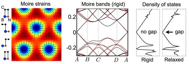
Image shows a graphene, a single-atom-thick sheet of carbon atoms arranged in a honeycomb-like lattice is one of the simplest materials with unrivalled mechanical and electronic properties. When placed on hexagonal boron nitride, a wide bandgap insulator, there is a significant buildup of atomic-scale strain (left panel). If graphene remains rigid, it remains a conductor (middle-panel), but allowing for the carbon atoms to relax makes the heterostructure a high-quality semiconductor (right panel). [Image credit: Jeil JUNG]
Reference
J Jung, AM DaSilva, AH MacDonald, S Adam “Origin of band gaps in graphene on hexagonal boron nitride.” Nature Communications 6 (2015) 6308 doi:10.1038/ncomms7308